
For this example we used the:
- NUCLEO-F401RE
- STM32CubeIDE (ver.1.3.1)
- The Reference Manual for STM32F401RE is here (RM0368)
- The Reference Manual of HAL/LL manual for STM32F4 library (UM1725)
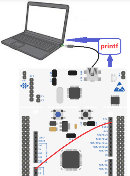
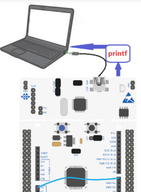
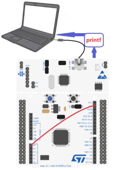
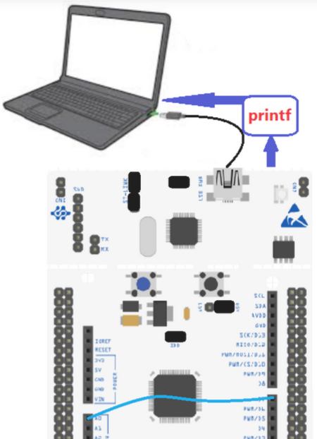
We display the result on the PC using Virtual Com port.
ATTENTION
Our sw use the huart2 that is the handler of the USART2 that is connected to ST-LINK emulator for exit like a virtual com.
Normally on the:
64pin NUCLEO is used the USART2 (huart2) but,
on 144pin NUCLEO, the USART is USART3, so the handler to use is huart3.
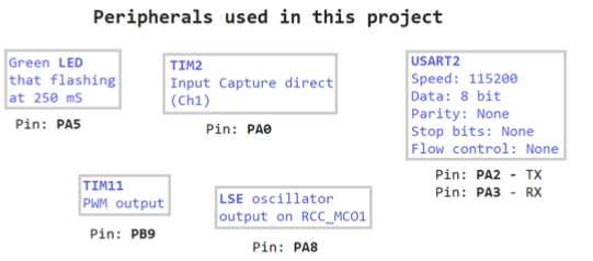
The below red wiring is for connect the PWM output of TIM11 (PB9)
with the CAPTURE input of TIM2 (PA0).
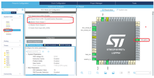
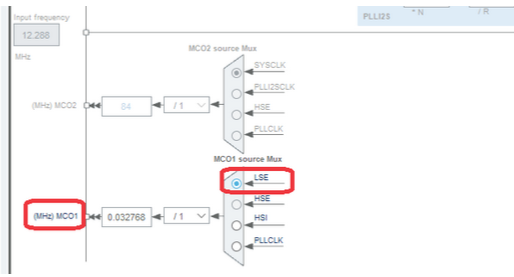
The below blue wiring is for connect the LSE oscillator output RCC_MCO1 (PA8)
with the CAPTURE input of TIM2 (PA0) .
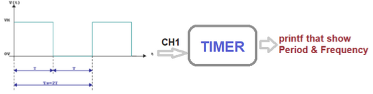
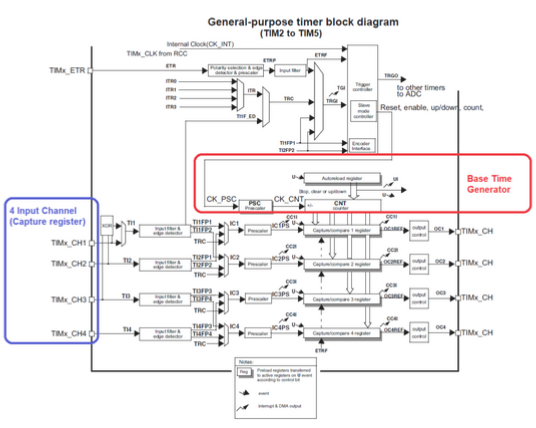
For use CAPTURE functionality we use the TIM2 and the Input Capture for measure two sequential transaction (from 0 to 1) by the relative Input Compare Pin (PA0) (Input Signal, CH1…CH4) for calculate the period and frequency.
NOTE:
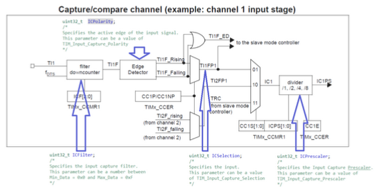
The INPUT FILTER & EDGE DETECTION
is useful for filter the input (de-bouncing) and for decide the polarity of the transaction that you need to detect (0 to 1 or 1 to 0).
NOTE:
The CAPTURE/COMPARE register is only ONE for each channel so is necessary read it after any trigger of input signal.
In fact the TIMER generate an interrupt every Input Capture trigger.
- The COMPARE is for the OUTPUT block (oc1…oc4)
- The CAPTURE is for the INPUT block (CH1…CH4)
Working principle
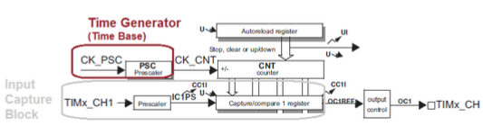
Below there is the a simplify TIMER block diagram.
NOTE:
The external period or frequency are not measured directly from the timer but is an STM32 computation.
Suppose that we setup the TIM with a time base (Time Generator) at 1KHz, the time resolution is 1mS (1/1000=0,001).
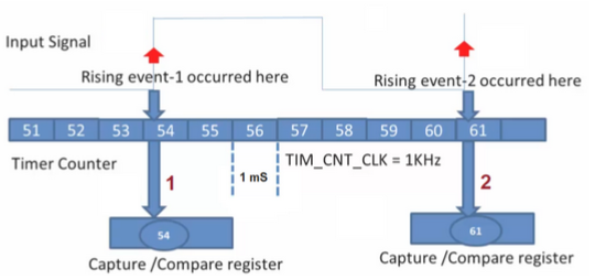
Each time the CAPTURE is triggered, an Interrupt (or callback) is generated which we will use to save the value contained in the register: CAPTURE (1, see below).
The next time the CAPTURE input is triggered, we will do the same procedure again, saving the new value contained in the CAPTURE register (2, see below ).
See the below image.
Now for calculate the Time Period you must do simply the difference from the previous values acquired, in our case: 61-54 that is 7.
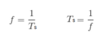
We know that our resolution is 1mS so out Time Period (Ts) is 7mS.

To conclude, below the formulas of Frequency and Period (Ts).
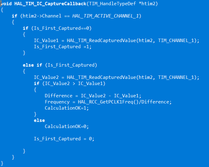
For read the CAPTURE register of TIM2 we use the below callback inserted from:
/* USER CODE BEGIN 4 */
and
/* USER CODE END 4 */
NOTE:
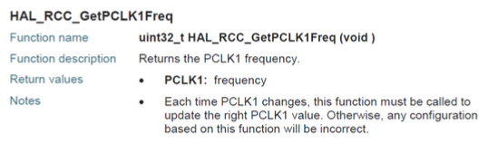
For read the time base of our TIM2 (for calculate the frequency) we use the function below, see the HAL/LL manual of STM32F4 library (UM1725).
Practical implementation
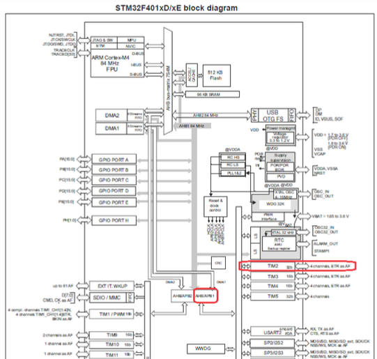
As you remember, we decided to use the NUCLEO-F401RE, below there are the configuration to do in STM32CubeIDE.
Formula:
The minimum frequency that the Timer can read is equal to:
TIMx CLOCK/ARR
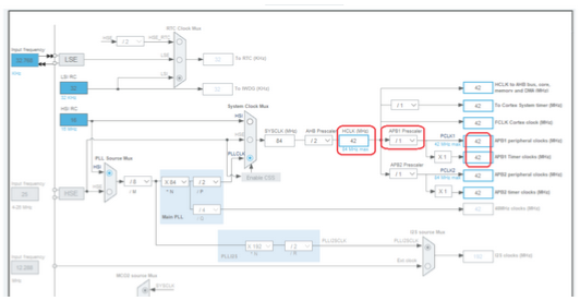
TIMx CLOCK depend of your configuration, in our case is 42 MHz.
In our case the minimum frequency measurable will be:
42MHz/65536 = 640 Hz
See below how to configure the Clock.
See below for configure the LSE oscillator and it’s output.
Configure the TIM2 (input CAPTURE mode) for reading pin PB0, see below.
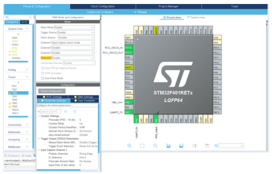
Below an explanation image concerning the Capture parameters.
The ICFilter is for filter (debouncing) your input channel.
In a real application we suggest to use a filter (ICFilter) for debouncing the signal that you need to measure.
The ICFilter is a digital filter is made of an event counter in which N consecutive events are needed to validate a transition on the output, see the Reference Manual of the STM32 that you use, in our case (STM32F401) is the here (RM0368).
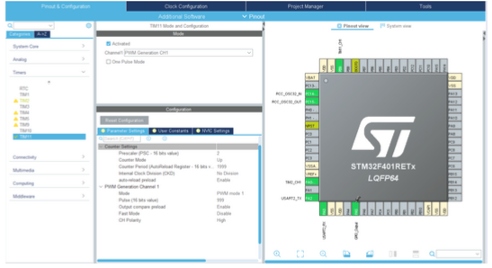
Configure the TIM11 (for generate PWM on pin PB9),see below.
We also need configure the USART2 for use it via the emulator, that is present on 64 pin NUCLEO board, like a Virtual Com through the USB port.
For the way to use the Virtual Com and printf see this explanation.

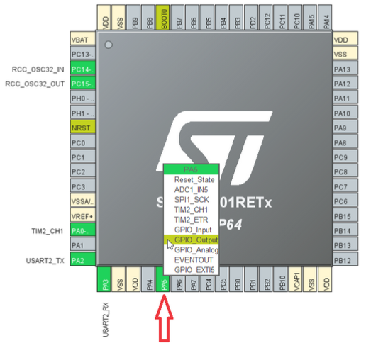
Again we need to use also the PA5 for flash the green LED present on NUCLEO board.
Now is necessary:
- Start the TIM11 for generate a PWM (7 KHz on pin PB9,– for PWM description see here) to use in input to TIM2 pin PA0
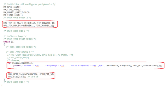
- Start the TIM2 by using the command: HAL_TIM_IC_Start_IT(&htim2, TIM_CHANNEL_1);
- Start the TIM11 by using the command: HAL_TIM_PWM_Start(&htim11, TIM_CHANNEL_1);
- Flash the LED (PA5)
See below.
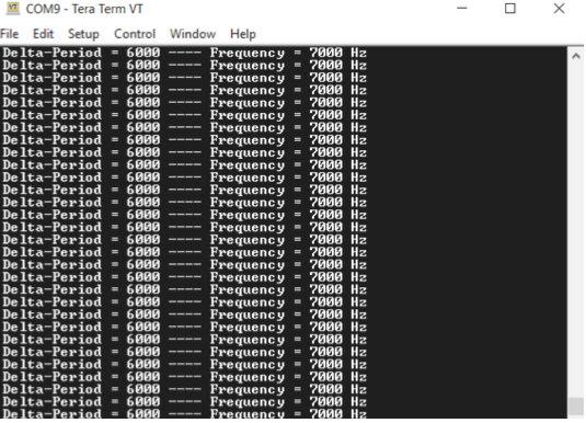
On Tera Term you must see something like below if you connect PWM output of TIM11 (pin PB9) with the CAPTURE input of TIM2 (PA0).
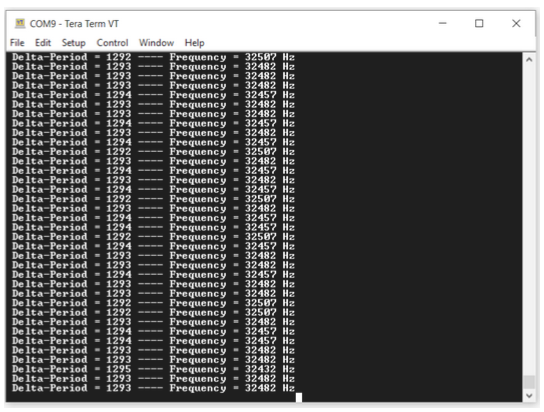
On Tera Term you must see something like below if you connect LSE oscillator output RCC_MCO1 (pin PA8) with the CAPTURE input of TIM2 (PA0).
CAUTION:
The accuracy of the frequency reading may not be high because we have used the HSI oscillator which in itself is not very precise.
In addition, there is the error due some noise present on the output PA8 of LSE (if you use it) and to the supply voltage and the resolution of the timer.
How to get the SW for this project
Please send us an email and ask us the password for: TimPeriodFreq
Please specify also your country and your city, this are only for our personal statistics.
Get the SW clicking here, but remember to ask us the password for open it.
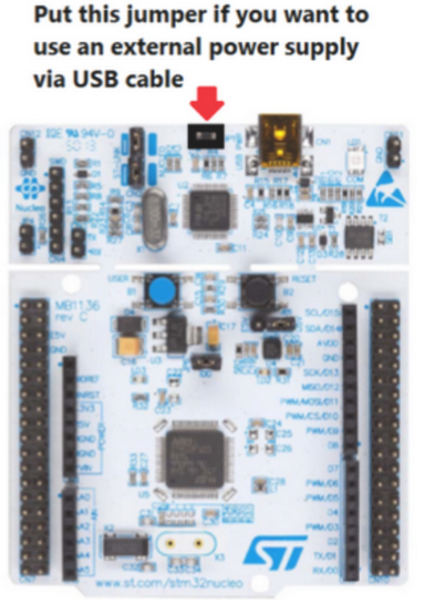
Power Supply NOTE:
NOTE:
- Use FIREFOX or CHROME for a clear view of the images present in this web site
- For enlarge the image press: CTRL +
For reduce the image press: CTRL –